A full wave rectifier that converts alternating current (AC) to pulsating direct current (DC) can be form by using two or four power diode connected to a single load resistance (RL) with each diode taking it in turn to supply current to the load. If you know about rectifier, than you know to reduce the ripple on direct DC voltage by connecting capacitor across the load resistor. This is use for low power applications, but not for smooth DC supply applications. One method that improves the smooth DC voltage of every half cycle waveform knows a full wave rectifier (FWR). In this tutorial we are going about the full wave circuit, working of circuit and VI characteristics.
What is a Full Wave Rectifier?
A full wave rectifier is a diode and resistor circuit that converts the both halves of each cycle of an alternating wave into pulsating DC signal. Full wave rectifiers that converts alternating voltage to DC voltage using two or more diode. That circuit is rectifier whose convert alternating current to direct current. If such rectifiers rectify both positive and negative of alternating wave is called a full wave rectifier circuit. A full wave rectifier is made by using two or more diode. Diodes conduct in only one direction. We use this principle of diode to construct full wave rectifier circuit.
Types of full wave rectifier
The rectifier circuits are manly two types which are given below. When we use two diodes is called half wave rectifier and when we use two or four diode is known as bridge rectifier.
- Half Wave Rectifier
- Full Wave Rectifier
When we use half wave rectifier, most of power gets wasted because it only conducts for one half cycles and other half cycle gets blocked. Efficiency of half wave rectifier is only 40.6% and we can’t use it for those applications that need a smooth and study output. Full wave rectifiers is a more efficient and study DC output as compare to half wave.
Full Wave Rectifier Theory
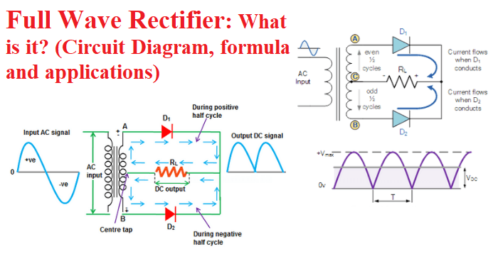
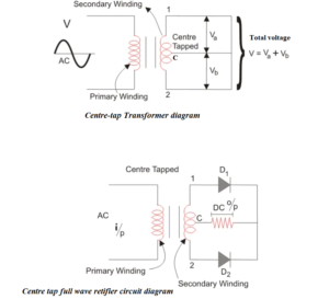
In full wave rectifiers circuit, we use two diodes for rectifications, one diode for positive half cycle and other is for negative half cycle of alternating wave. Full wave rectifiers circuit uses a multiple winding transformer whose secondary winding is split into two equal halves with a common center tapped connection. Each diode conducts when its anode terminal is positive with respect to center point “C’ of the transformer and the output will produce during both half cycles.

The full wave rectifier circuit consists of two power PN junction diode and the diode output terminal is connected with load resistance (RL) with each diode taking it in turn to supply current to the load. In secondary winding, the point A is positive with respect to point C, the diode D1 is forward bias as indicated by the arrow.
When point B is positive with respect to point C, the diode D2 will start conducts and the current flowing through resistor R is in the same direction for both half cycles. The output voltage across the load resistor is the phasor sum (180° + 180°= 360°) two waveforms combined. The full wave rectifier is also called as a “bi-phase” circuit.
The full wave rectifier is further classified into two categories:
- Centre-tapped Full Wave Rectifier
- Full Wave Bridge Rectifier

Centre-tapped Full Wave Rectifier
Construction of Centre-tapped Full Wave Rectifier
A center tap rectifier is a two diode type rectifier and this system consist of
- Centre-tapped Transformer
- Two Diodes
- Resistive Load
Centre-tapped Transformer: – It is a conventional type of transformer except the secondary winding is split into two equal parts.
This center tap rectifier voltage is divided into two equal and opposite polarity, namely +Ve voltage (Va) and -Ve voltage (Vb), and total voltage is V=Va + Vb. circuit diagram of center tap rectifier is given below:
Working of Centre-tapped full wave rectifier
Now we are going to discuss the working of Centre tapped rectifier, we apply an alternating wave (AC) to primary winding of the transformer. The AC supply is high so, we use step down Centre-tapped rectifier. When the positive cycle of the AC voltage is arrive, terminal 1 will be positive with respect to terminal 2, and the Centre-tap will be at zero potential.
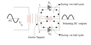
When the terminal 1 is positive the diode D1 will be forward bias and current flow through load resistance. D2 will be reverse bias.
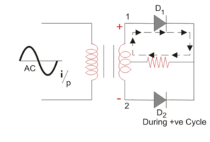
During negative half cycle terminal 2 will be positive with respect to terminal 1 and Centre-tap will be zero potential. Due to this the diode D2 will be forward bias and it will conduct for negative half cycle. The diode D1 will be reverse bias so it will not conduct.

When terminal 1 is positive with respect to the terminal 2 the diode D1 conducts and when terminal 2 is positive with respect to the terminal 1 the diode D2 conducts. The both half cycle are passes through resistor.
Output waveform of Centre-tapped full wave rectifier
In Centre tapped rectifier, the diode D1 will work only for positive half cycle and diode D2 will be work only for negative half cycle of alternating wave the waveform of Centre tapped rectifier is given below.

Filter Circuit
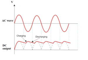
The full wave rectifiers produces a pulsating direct currant and we can’t use this pulsating DC for practical application. So, we convert pulsating DC into pure DC voltage. We can achieve pure DC by using filter circuit and this circuit is shown below. In filter circuit the capacitor is place across the load resistance.
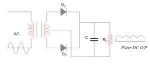
The property of capacitor filter is short the ripple and block the DC component. When we applied AC voltage more than the capacitor voltage, the capacitor will start charge and achieve immediately to the maximum value of the input voltage. Hence input voltage is equal to the capacitor voltage.
When the AC input voltage start decreasing and less than the capacitor voltage, the capacitor start discharge at low rate and the capacitor is not fully discharge because another wave will come and again charge the capacitor. The capacitor will discharge when negative cycle came and the above process happens again.
Full Wave Bridge Rectifier
Construction of Full Wave Bridge Rectifiers
A bridge rectifier is a that type in which the four power diode this circuit consist of stem consists of
- Four power diodes
- Resistive Load
We can mention the name of diode is A, B, C and D. below the figure shows the bridge rectifier.

Principle of Full Wave Bridge Rectifier
When we apply AC input to bridge rectifiers, during the positive half cycle the terminal 1 is positive with respect to the terminal 2. Due to this the diode A and C will be forward bias and it will conduct and output. The diode B and C will be reverse bias during this time. The path of currant flow is 1 to 4 and 3 to 2.

When negative cycle arrives the terminal 1 is become negative and terminal 2 become positive. This will cause the diode B and D forward bias and rest diode will be reverse bias. The path of currant will be 2 to 4 and 3 to 1.

And the output waveforms are given below. In these waveforms the diode A & C will conduct for positive half cycle and the diode B & C will conduct for negative half cycle.

Full Wave Rectifier Formula
Now we are going to derive the various formula of full wave rectifier.
Peak Inverse Voltage
Peak inverse voltage (PIV) is the maximum reverse bias voltage across a diode can withstand in before breakdown.
The PIV for full wave is 2Vmax and it is double of the half wave.
DC Output Voltage
The following formula helps to find out the average value of DC
Vdc = VdcRL = (2/π)Imax RL
RMS Value of Current
Irms = Imax /√2
Form Factor
Kf = (RMS value of current / average value of current) = Irms/Idc = {(Imax /√2)/ (2Imax /√ π)} = 1.11
Form factor of Centre tapped rectifier is 1.11
Rectification Efficiency
η = (DC output power /AC output power)
Efficiency of Centre tapped rectifier is 81.2%
Ripple Factor of a Full Wave Rectifier (γ)
formula of Ripple factor of full wave is
![]()
Ripple factor of full wave is γ = 0.48
Advantages of Full Wave Rectifiers
- The efficiency of full wave is higher than half wave. This means that they convert AC to DC more efficiently.
- Power loss is low because no wastage of voltage.
- It has low ripple factor.
Disadvantages of Full Wave Rectifiers
- It is more expansive then half wave rectifier.