The PIN diode is slightly different from the conventional type of PN junction and it is use in particular applications. The slightly differ is is another type of diode that is undoped and wide intrinsic semiconductor region between P and N layer. In PIN diode the P and N region is heavily doped region. The pentavalent doping impurity is added in N region and trivalent impurity is added in P type region. The wider intrinsic region is the major difference of ordinary PN junction diode. This region makes the diode an inferior rectifier. This component is always available in fast switches, attenuators, photo detectors and high voltage power electronics applications.
 What is a PIN Diode?
It is a special type of diode. It contains three layers that are P-type, I-type and N type layer. The intrinsic semiconductor (I- type) layer is place in between the P-type semiconductor and N-type semiconductor. It is slightly different in ordinary PN junction because of extra one layer is present. The intrinsic layer is crystal of silicon or germanium without any doping in it. Intrinsic layer not conduct electric current well. The doping level of P and N layer is high and they are used for ohmic contacts. The current through it follow P region, intrinsic region and then an N region, thus making it a PIN diode.

This diode is kind of photo diode that is use to convert light to electrical energy.
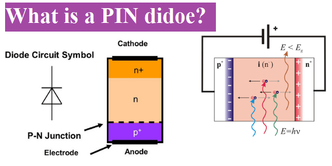
PIN Diode Symbol
It has two terminals that are anode (A) and cathode (C). The anode terminal is a positive and cathode is negative terminal. The symbol is shown below. It symbol is almost same to ordinary PN junction except the straight line present at mid of the triangle which is shown in figure.
Construction of a PIN Diode
The structure of PIN diode same as ordinary PN junction and its structure is shown below. This includes three layers of semiconductor material that are P-type, N-type and intrinsic type of layer but in ordinary PN junction has only two layer P and N semiconductor layers. The intrinsic semiconductor is a purest form of semiconductor and P, N is the impure form of semiconductor. In N-type semiconductor the pentavalant impurity addition and P-type semiconductor is form by addition of pentavalnat impurity. And no any impurity is present in intrinsic layer.

The construction of PIN diode is done by two methods one is planar structure and another is mesa structure. In planar structure, A P region can be formed through a thin epitaxial layer by forcing it over the intrinsic layer. Likewise, the N region is formed opposite of the P region. The resistivity of intrinsic layer is 0.1Ω-m. This is high resistive. In the mesa structure, the semiconductor is doped previously on the intrinsic region. So, that PIN diode can be formed.
Working of the PIN Diode
The PIN diodes is almost similar to the conventional PN junction. Only difference is that one extra intrinsic layer is present at the center of P and N region. PIN diodes is an inferior rectifier but is widely use in attenuators, switches, etc.
Forward biased operation
When P side is connected to the positive terminal of the battery and N region is connected to the negative side of batter. It becomes forward bias and the depletion region at the p-n junction reduces. With the reduction of the depletion region current start flowing through diode. The behavior of PIN diode is like a variable diode when it is operated in forward bias. In forward bias operation a high electric field is produce across the junction and speeds up the transport of charge carriers from the P region to the N region. Due to this diode is operated fast, so it is use in high speed switching and high-frequency applications.
Reverse biased operation
When we reverse the forward connection than diode become reverse bias operation. The width of depletion region of PN junction starts increase. We further increase the reverse voltage, width of depletion region is increases as far as whole mobile carriers swept away from the intrinsic region. This particular voltage is called swept out voltage. Usually, its value is -2V.
Characteristics of PIN Diode
At reverse voltage the depletion layer becomes fully depleted. The capacitance is not dependent on the level of bias once the depletion layer is fully depleted. Due to this small charge is in intrinsic layer. The leakage of RF signal is lower than other PN junction because the level of capacitance is typically lower.
In forward bias, it is behaves like a variable resistance and no rectification or distortion. The variable resistance value is dependent on the forward bias voltage. Some short point of its characteristics is described below:
- The capacitance is independent of bias level as the net charge is said to be very less in the intrinsic layer
- It possesses very low reverse recovery time
- It obeys standard diode equation for all the low-frequency signals.
- It appears like a resistor than any other non- linear devices and is said to produce no distortion or rectification.
Application of PIN Diode
Pin diodes have many applications. Some of the application is given below.
- RF switch: It is use in RF switch. The intrinsic layer is present at the center of P and N region the level of capacitance When the reverse voltage is increases the depletion region is increases. This makes it an ideal RF switch.
- High Voltage Rectifier: The presence of intrinsic layer in between P and N region that increase the distance between P and N and thus allowing higher voltage tolerance between junctions.
- Photodetector: The PIN diode is use as a photodiode when depletion region is increase. This increment increases the volume of conversion and efficiency of the photodiode too.
- It is use in X-ray and gamma rays photons.
- It uses in to protect RF circuit.
Advantages of PIN:
- Low noise
- Low dark current
- Low bias voltage
- Higher reverse voltages to be tolerated
- High-speed response
- Low junction capacitance
- Large depletion region
Disadvantages of PIN:
- Less sensitivity
- No internal gain
- Small area
- Slow response time
- High reverse recovery time due to power loss are significant
Some important point about PIN diode
The key performance parameters such as Frequency range, bandwidth, Repeatability, isolation, Operating life, and power handling are shown in tabular form below. The RF switches is based on solid-state components of PIN diodes, FETs, and hybrid devices as well as electromechanical implementations.
| Parameter | Solid state switches | Electromechanical switches | ||
| Pin diode | FET | Hybrid | ||
| Frequency range | from MHz | from DC | from kHz | from DC |
| Intersection loss | Medium (Roll off at low frequencies) | High (Roll off at high frequencies) | High (Roll off at high frequencies) | Low |
| Isolation | Good at high frequencies | Good at low frequencies | Good at high frequencies | Good across broad frequency range |
| Repeatability | Excellent | Excellent | Excellent | Good |
| Switching speed | Fast | Average | Average | Slow |
| Power handling | Low | Low | Low | High |
| Operating life | High | High | High | Medium |
| Power consumption | High | Low | Moderate | Current interrupt feature reduces current consumption |
| Sensitive to | RF power overstress, temperature | RF power overstress, temperature | RF power overstress, temperature | Vibration |
| Agilent switch examples | P9400/2/4 85331/2 |
U9397, U9400 | L series, 8710x/20x | |
Representative maximum and minimum levels for the three classes of solid-state switches cover a wide set of overlapping ranges as shown in Figure.
| PIN diode switches | FET switches | Hybrid switches | |
| Lower frequency limit* | 100 MHz | DC | 300 kHz |
| Upper frequency limit* | >50 GHz | >20 GHz | >20 GHz |
| *Typical. Based on performance requirements. | |||
Also read:– Schottky diode, Type of diodes, Tunnel diode.
PIN Diode Questions (FAQs)
Name the material that is used in the PIN diode.
The material use in PIN diode is Silicon because its power handling capacity high.
How many layers of semiconductors are there in PIN diode?
The number of layer of semiconductor is three P-type, N-type and intrinsic type. The size of intrinsic layer is thicker than other two layer.
What happens to the resistance of the PIN diode with a positive bias voltage?
It decreases.
What is the forward resistance of the PIN diode?
RF =W/σN
The forward resistance depends on the current density, positive charge carrier concentration and width.
What is the value of forward current in frequency models?
IF=A(μPP+μNN)q
Where,
μP → Mobility of p-type charge carriers
μN → Mobility of n-type charge carriers.
What happens in the PIN diode for low-frequency model?
At low frequency the resistance is decreases and reactance is increases.
When does the PIN diode act as a variable capacitor?
When the diode is connected in reverse bias configuration, it acts as a variable capacitor.
When does the PIN diode act as a variable resistor?
When it is in forward bias configuration, it acts as a variable resistor.
What is a PIN diode used for?
It is use in current-controlled resistors at RF and microwave frequencies, with low resistance when it is forward bias approx few ohm and high resistance offers in reverse bias approx 10k Ω
What is the principle of PIN diode?
The principle of PIN diode, it is a variable resistance when it is forward bias. When it is forward bias the high electric field develop around the junction and that electric field speed up the electron transportation from P to N region. Due to speed moment of electron, it is used for high-frequency applications.
What is the full form of PIN diode?
The Acronym for positive-intrinsic-negative diode. A photodiode with a large, neutrally doped intrinsic region sandwiched between p-doped and n-doped semiconducting regions.
What Is PIN diode junction?
It is a special type of diode. It has only three layer and that are P-type, I-type and N type layer. The intrinsic semiconductor (I- type) layer is sandwiched between P-type semiconductor and N-type semiconductor layer. It is widely use in microwave applications.
What are the three layers of PIN diode?
This diode contains three layers of semiconductors. The three layers naming P-type layer, Intrinsic layer and N-type layer. The intrinsic region is present in between P and N layer.