A diode is generally known as on direction current follow device. A Zener diode is a heavily doped diode. The purpose of heavily doping is to operate in reverse direction without any damage. When zerer diode connected in reverse direction to the supply and increases the potential increase at a certain level. When reverses voltage reach certain level at which junction brakes down and the current flows in the reverse direction and other word Breakdown voltage at zener start conduction in reverse direction, this phenomena is called zener effect,
Zener diode Definition
Zener diode is a special diode which is made of semiconductor material. It allow the current follow to the backward direction. When it is set to certain reverse voltage know as Zener voltage. It is heavily doped p-n junction diode work in reverse direction without failing completely. Due to heavily doping the depletion region is very thin and electric field is very high. The width of depletion region in order to10-6 (approx) and the range of high electric field is 5*106 voltage/meter (approx). It is use as voltage regulator. When it is forward bias it behaves just like a convectional diode passing the rated current. It is very useful electronics component and widely used in electronics circuit.
However the conventional diode block the reverse voltage but the Zener begins to conduct in the reverse direction. The reason behind is when a reverse voltage applied across the Zener and exceeds the rated voltage. Due to exceed voltage Avalanche Breakdown occurs in the depletion layer and current flow through the diode. It is use in stabilized power supply rails to provide reference voltages for circuits. They are also used and also use to protect circuits from high voltage, especially electrostatic discharge. The name of Zener diode was introduce after the discovered Zener effect by the American physicist Clarance Melvin Zener.
Zener diode symbol
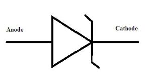
The symbol zener is very similar to conventional p-n junction diode except only difference is bent edges on the vertical bar. The Zener diode symbol consists of anode and cathode terminal the anode terminal is +ve terminal and the cathode is the –ve terminal. It operate in both direction these are forward bias and reverse bias. Mainly it is operated in reverse bias direction.
Zener diode circuit
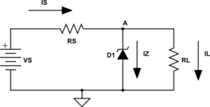
Normally we use the Zener diode circuit in reverse direction. When it is using forward direction it behaves like a convectional diode. the cicuit configuration are the diode is connected in reverse bias which is done by connecting of anode is to the –ve terminal of power supply and cathode is connected to the +ve terminal of the power supply. This circuit contains resistance, Zener diode and power supply. The current through diode is IZ and the current through resistance IS & IL which is labeled in figure.
Zener diode working
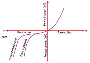
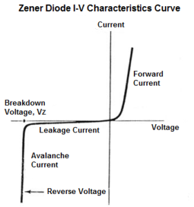
ON state – when the reverse voltage across the Zener is equal or greater than the breakdown voltage, the current is increasingly sharp. In this region the curve of current is almost vertical. It means the voltage across the Zener is almost constant even through the current changes. The ideal Zener diode in breakdown region can be represented by battery voltage.
OFF state- when the reverse voltage across the Zener is less than the breakdown voltage but it has some voltage, it is in OFF condition. Diode is act as an open circuit.
How does a Zener Diode work in reverse bias?
The behavior of zener diode in forward direction is same as normal PN junction diode. However, when connected in reverse bias, a small leakage current follows through zener. The order of small leakage current is in micro ampere. As the reverse voltage increases to the predetermined breakdown voltage (Vz), current starts flowing through the diode. The currnet reach maximum value and this maximum value is determin by series resistor. After a certain point the current get stabilizes or constant over a wide range of applied voltage.
There are two types of breakdowns for a Zener Diode:
- Avalanche Breakdown
- Zener Breakdown
Avalanche Breakdown in Zener Diode
Avalanche effect comes in normal diode and zener. In avalanche effect the reverse voltage is high. When high reverse voltage is applied across the PN junction the free electrons gain high energy and these electron accelerate at high speed. The high movement of electrons collide other atoms and knocks off more electrons. This continuous collision process generates a large no of free electron. The generation of electrons produce large amount of current. The sudden increases of electric current permanently destroy the convention PN junction. We need a zener diode at which operates under the avalanche breakdown.
Zener Breakdown in Zener Diode
When we applied a reverse bias voltage reaches closer to zener voltage, in depletion region the electric field get strong to pull out electron from the valance band to conduction band and create free electron. This free electrons, in turn, give rise to a high value of reverse saturation current. This is known as Zener breakdown. At Zener breakdown, a low increment in voltage gets a rapid increment in current.
The graph show’s the Avalanche Breakdown Zener Breakdown
V-I Characteristics of Zener Diode
V-I characteristics divided into two region
- Forward region
- Reverse region
Forward region
When the –ve terminal of batter is connected to the anode of the and the –ve terminal of the supply is connected to the cathode, than the diode is called forward bias. In forward bias region the diode act as conventional diode characteristics.
Reverse region
When the anode terminal of the diode is connected to the –ve terminal of the supply and the cathode terminal of the diode is connected to the +ve supply diode is called reverse bias. The Zener become in reverse bias region, below the Zener voltage (Vz) it has some current. This current is produce by the minority carriers. If we further increase reverse voltage the reverse current is increases sharply, this indicates the breakdown voltage occurred. This is called breakdown voltage or Zener voltage and it is indicated by Vz. The reverse voltage after the Zener voltage (Vz) is almost constant.
Zener Diode Specifications
Some commonly used specifications for Zener diodes are as follows:
Zener/Breakdown Voltage – The reverse breakdown voltage of zener diode lie from 2.4 v to 200 v. Some time it increases maximum value from 1kv.
Current Iz (max) – It is the maximum current rating which is from Vz – 200μA to 200 A.
Current Iz (min) – Minimum currant for the diode go to breakdown.
Power Rating – maximum rating of power. It is the product of zener voltage and zener current.
Temperature Stability – Diodes around 5 V have the best stability
Voltage Tolerance – It is typically ±5%
Zener Resistance (Rz) – It is the resistance to the Zener diode exhibits.
Applications of Zener Diode
It is mostly use in industry and commercial application like voltage regulator. The some application of zener diode is described below.
- As Voltage Stabilizer:- The zener diode provided constant voltage in a circuit from fluctuating from voltage source to load. This is connected in reverse bias and parallel with load when it obtains knee voltage it will provide a constant voltage in circuit.
- Zener diode in overvoltage protection:- If input voltage is higher than breakdown voltage, the current flow through diode and voltage drop across resistor. This voltage drop will trigger the SCR and as a result from shorts circuit with ground. The short circuit opens up the fuse and hence it then disconnects the load from the supply. The zener diode over-protection is use in multimeters.
- For Wave Shaping:- The zener diode is use to convert sine wave to square wave. And this is done by connecting two diodes in opposite direction. The combination of two diode is in series with resistance.
- It is used as voltage reference.
- Voltage stabilizers or shunt regulators.
- Switching operations.
- Clipping and clamping circuits.
Advantage
- Power dissipation capacity is very high.
- Low cost.
- Accuracy is high.
- Small in size.
Disadvantage
- This is not sutable for large load current
- The zener resistance slightly changes DC output.
- The circuit has high internal impedance
- Changes within load current generate changes within Zener current.
- The adjustment of the output voltage cannot be done.
Summery
This tutorial is about of zener diode and its principle. This is work only in reverse bias because in forward bias it behaves like a normal PN junction diode. This diode is mostly use in both commercial and industrial field. Some of them are like a Stabilizer or Voltage Regulator, Meter Protector & Wave-Shaper.
People also ads about Zener diode:-
What is Zener diode and its function?
The zener diode is semiconductor device that are heavily doped as compare with normal diode. The region behind of heavily doped is this diode can be use in reveres bias at certain voltage without any damage.
What is principle of Zener diode?
Zener Diode Working Principle
When the didoe is conncted in forward bias the currnt start flow through and when it is in reverse bias the current will not flow through it. This voltage has surpassed the breakdown point (in reverse bias), the diode falls in the Zener region, where it conducts without getting damaged. Current in this region is called avalanche current.
Where is Zener diode used?
The zener diode is widely use in domestic and industrial. The some use of zener diode is Zener diode in overvoltage protection,As Voltage Stabilizer and For Wave Shaping.
What is Zener diode characteristics?
The characteristics of zener diode are same as conventional diode. The diode is turn ON voltage is 0.3 to 0.7.
What is the difference between normal diode and Zener diode?
The diode is made of semiconductor material which is use as a switch or conduct in only one direction. The conventional diode is conduct only one direction i.e. forward direction. And zener diode is also conduct both direction as well as forward and reverse direction but it is only use in reverse bias direction.
What are the advantages of Zener diode?
Advantages of Zener diode:
⇒ As Voltage Stabilizer ⇒ Zener diode in overvoltage protection ⇒ For Wave Shaping ⇒ voltage reference ⇒ Switching operations ⇒ clipping and clamping circuits.